Log #004: PCB Üretimi
Atığı Sanata, Kaosu Geometriye Dönüştürelim
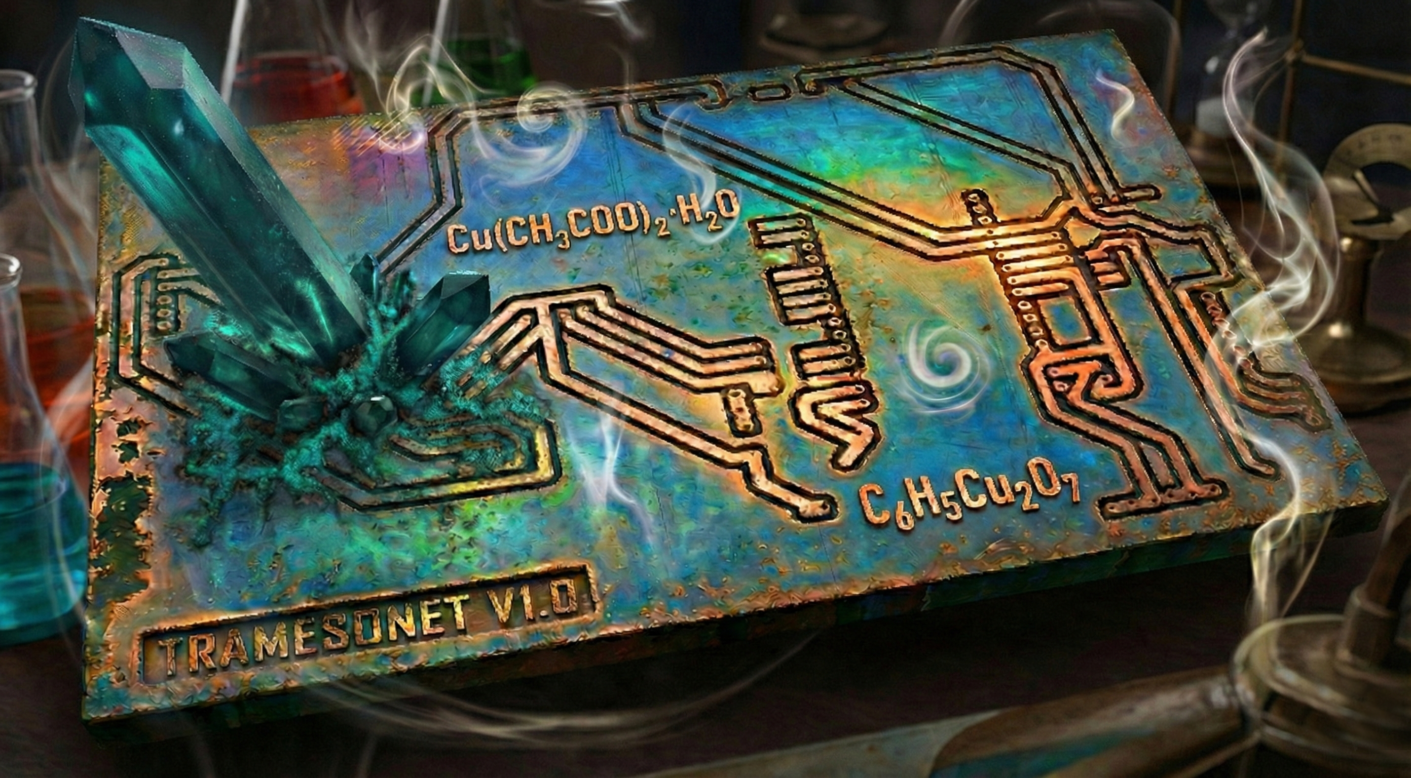
Meteoroloji istasyon ağı için süreç devam ederken olabildiğince “kendin yap” yöntemleri ile hikâyeme devam ediyorum.
Meteoroloji istasyon ağımız için, elbette önceki yazılarımızda da belirttiğim gibi, elektronik devre ve modüller olmazsa olmaz bileşenlerimiz arasında yer alıyor. Hazır yapılmış modüller kullanıyor olsak da bu modülleri bir araya getirmek için PCB denilen lehim yapılabilen malzemeleri kullanıyoruz. Bu modüllerin birbirleri ile haberleşmesinin stabil ve sürdürülebilir olması için lehim kullanılarak komponentlerin hem iyi bir iletkenlik kazanması hem de mukavemetli bir zemine oturtulması gerekiyor. Bunun için elektronikte sıkça kullanılan bakır elementi tercih ediliyor. PCB denilen plaketin üzeri çeşitli kalınlıklarda bakır ile kaplanıyor.
Bu plaketin üzerini çeşitli mürekkep yöntemleri ile örtüyoruz. Yalnızca devre elemanlarının birbirleri ile bağlı olmasını istediğimiz aralıkları örterek diğer yüzeyleri temiz bırakıyoruz. Bir çözelti içerisine atılan bu plaket, mürekkep ile boyanmış yerleri aşındırmazken; mürekkep sürülmeyen yüzeyleri ise eriterek iletkenliğini yok ediyor.
Sürecin aşamaları, EasyEDA isimli programın online sürümünde modüllerin birbirleri ile haberleşmesini sağlayacak taslak çizimlerinin yapılması ile devam etti. Çizimler bitince tonerli yazıcıdan, “baskı devre kâğıdı” olarak piyasada satılan parlak yüzeyli kuşe kâğıda çıktı alındı. Bu çıktı, plakete aktarılarak çözeltide banyo yaptırma sürecinin zeminini hazırlıyor. Çıktı aldığımız baskı devre çizimimizi plaketin boyutunda keserek ve bakır yüzeye kapatarak ütüleme işlemi yapıyoruz. Ütü sıcaklığı, toner tozunu kuşe kâğıdından kopartarak plaketin üzerine yapışmasını sağlıyor.
Eskiden okullarda gördüğümüz yöntem bu kadar kolay olmuyordu. Bu işlem için bilgisayar ve çizim programı kullanılmadan el ile çizim yapılıyordu. Ama sorun şu ki: El ile çizdiğiniz şekil bakır yüzeye kapatılınca ayna görüntüsü oluşturarak devre elemanlarının doğru şekilde yerleştirilememesine sebep oluyordu. Çözüm; baskı devre çizimini yaptığımız kâğıdı pencereye yaslayarak, ışığın yardımıyla kâğıdın arkasında beliren çizimin üzerinden tekrar geçmekle mümkün oluyordu. Dolayısıyla ayna görüntüsü alınmış olan kâğıdı kopya kâğıdı ile plaketin üzerine aktararak tekrar çizim yapılıyordu. Sonucunda plaketin üzerine doğru çizim aktarılmış oluyordu.
Tramesonet istasyon ağı, olabildiğince “kendin yap” odaklı ve açık kaynaklı bir proje. Projenin amacı; görece dar bir alanda, yüksek çözünürlüklü ve şiddetli hava olayları için erken uyarı sistemi olarak çalışmasıdır. Doğayı dinlerken ve ona cevap vermeye çalışırken çevreci bir tutumda olmayı görev edinmeliyiz. Bu yüzden istasyon ağımızın kalbi olan elektronik bileşenlerin PCB eritme sürecinde açığa çıkan atıklarımızı, sanatsal bir fenomene dönüştürmeyi hayal ediyorum. Aslında atığı sanata, kaosu geometriye dönüştüren mikro ölçekli bir fenomeni ortaya çıkaracağız. Mutfak malzemeleri ile kimya laboratuvarı kurmaya hazır mısınız?
Bakırın istenmeyen yüzeylerden kontrollü eritilmesi sürecini yukarıda anlatmıştık. Peki ama bakırı bu kadar hassas şekilde nasıl aşındırabileceğiz? Burada işin içine kimya giriyor. Kimya girerse sanat ve bilim de beraberinde gelir. Yani atığımızı mücevherlere dönüştüreceğiz. Orta Çağ simyacılarının iddia ettiği gibi değerli bir mücevher yaratamasak da atığımızı sanatsal bir görsele dönüştürmek bizim için aynı derecede kıymetli. İşin sonunda elde edeceğimiz mücevher ise: Bakır (II) Asetat Monohidrat kristali.
Bakırı çözdürmek için ihtiyacımız olan ve görece çevreye daha az zararlı olabilen malzemeler şöyle:
1
2
3
4
5
6
7
Hidrojen Peroksit (%50 H2 O2 ): Oksijenli su.

Sitrik Asit Monohidrat (C6 H8 O7 ): Limon tuzu.

Sofra Tuzu (NaCl): Katalizör olarak kullanılıyor.

Asetik Asit (%5): Beyaz sirke.
170×120×30 mm boyutlarında, sızdırmazlık ayarlarıyla 3D basılmış PLA kapta, bakırın bir kısmını çözdük. Bu işlemi kabı 10 dakikada bir hafifçe çalkalayarak yaklaşık 1 saat boyunca yapmaya devam ettik. Çözeltimizin rengi turkuaz-mavi tonlarına ulaştığında ve artık bakırı çözemeyecek doygunluğa geldiğinde yeterli kıvama geldiğini anlıyoruz.
Biraz hile yaptığımı kabul ediyorum; bakır plaketi hazırlarken çözdürücü solüsyonumun termal tepkimesi fazla olmaması için plaketi çok fazla tonerle örttüm (resimde bakır kaplı alanlar olarak görülebiliyor). Hal böyle olunca plaketin erimesi gereken bakır yüzeyleri eridi ancak çözeltim doygunluğa ulaşmadı. Ben de elimdeki bir miktar bakır elektrik telinden küçük parçalar ekleyerek, doğru renge gelene kadar çözdürmeye devam ettim.
Artık çözeltimizin rengi doyuma ulaştığını gösteriyor. Bir filtre yardımı ile çözeltimizi (Bakır II Sitrat) süzerek temiz bir kaba ayırdım. Bu sıvıya artık sıradaki malzememiz olan asetik asidi, yani sirkeyi ekleyebiliriz. Beyaz sirkeyi eklediğimiz çözeltimiz artık “Bakır (II) Asetat” oldu. Bu karışımı yayvan bir fincan tabağı benzeri bir kaba aldım. Yavaş buharlaşması için de üzerini hafif açık bırakarak örttüm. Tabağa ayırdığım bu küçük kısım, “tohum” üretmek için kullanılacak. Öte yandan, daha büyük bir kavanozda kalan çözeltimizi saklıyoruz; bu da kristal besini olarak sonrasında kullanılacak.
Kristallerimiz tohum oluşturup büyümeye devam ederken, biz sonraki yazımızda plaketimizin deliklerini delip lehimleme işlemlerine geçmeye başlayabiliriz.
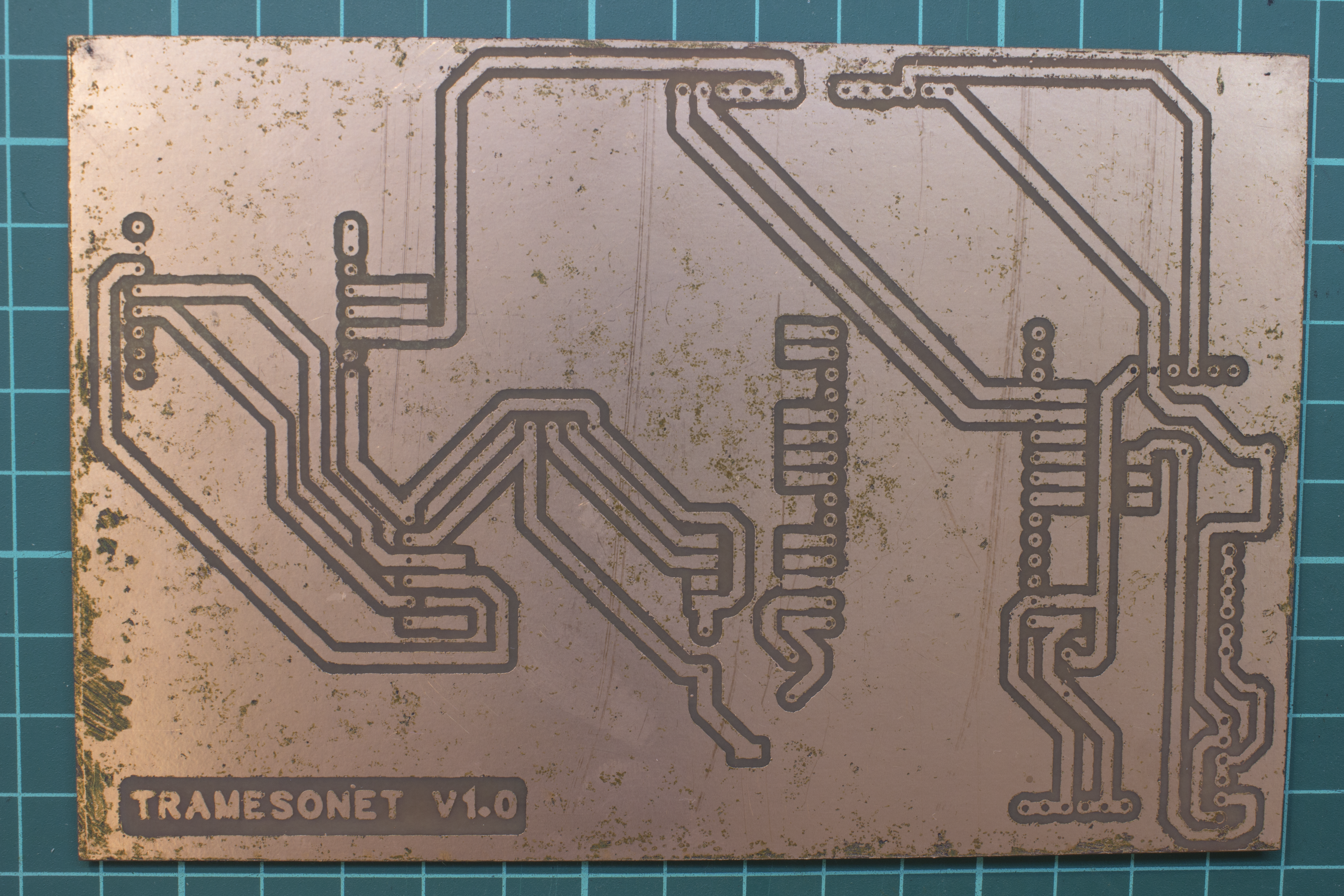
English Version While the process for the meteorology station network continues, I am moving forward with my story using “do-it-yourself” methods as much as possible.
As I mentioned in our previous posts, electronic circuits and modules are of course among our indispensable components for our meteorology station network. Even though we use ready-made modules, we use materials called PCBs, which can be soldered, to bring these modules together. In order for the communication of these modules with each other to be stable and sustainable, the components need to be placed on a grounded surface with both good conductivity and strength by using solder. For this, the element copper, which is frequently used in electronics, is preferred. The surface of the plate called PCB is coated with copper in various thicknesses.
We cover the surface of this plate with various ink methods. We cover only the intervals where we want the circuit elements to be connected to each other and leave the other surfaces clean. This plate, thrown into a solution, does not corrode the places painted with ink, while it dissolves the surfaces where ink is not applied, eliminating its conductivity.
The stages of this process continued with the creation of draft drawings using the online version of the program named EasyEDA in a way that would allow the modules to communicate with each other. When the drawings were finished, a printout was taken from a toner printer onto glossy couché paper, which is sold on the market as “printed circuit paper.” This print is transferred to the plate, preparing the ground for the bath process in the solution. We perform the ironing process by cutting our printed circuit drawing in the size of the plate and closing it onto the copper surface. The iron temperature ensures that the toner powder is detached from the couché paper and sticks onto the plate.
In the past, the method we saw in schools was not this easy. For this process, drawing was done by hand without using a computer and drawing program. But the problem was this: the shape you drew by hand created a mirror image when closed onto the copper surface, which caused the circuit elements not to be placed correctly. The solution was possible by leaning the paper on which we made the printed circuit drawing against the window and re-drawing over the drawing that appeared behind the paper with the help of light. Therefore, the drawing was made again by transferring the paper, of which the mirror image was taken, onto the plate with carbon paper. As a result, the correct drawing was transferred onto the plate.
Tramesonet station network is a “do-it-yourself” and open-source project as much as possible. The aim of the project is to work as a high-resolution severe weather event early warning system in a relatively narrow area. While listening to nature and trying to respond to it, we should adopt an environmentalist attitude as a duty. Therefore, I dream of transforming our wastes, which are released during the PCB etching process of electronic components that are the heart of our station network, into an artistic phenomenon. In fact, we will reveal a micro-scale phenomenon that transforms waste into art and chaos into geometry. Are you ready to set up a chemistry laboratory with kitchen supplies?
We have explained the process of controlled etching of copper from unwanted surfaces above. But how will we be able to etch copper so precisely? This is where chemistry comes in. If chemistry enters, art and science come with it. In other words, we will transform our waste into jewelry. Even if we cannot create a precious jewel as medieval alchemists claimed, transforming our waste into an artistic visual is equally valuable for us. The jewel we will obtain at the end is: Copper (II) Acetate Monohydrate crystal.
The materials we need to dissolve the copper and which can be relatively less harmful to the environment are as follows:
1
2
3
4
5
6
7
Hydrogen Peroxide (50% H2 O2 ): (Oxygenated water)

Citric Acid Monohydrate (C6 H8 O7 ): (Lemon salt)

Table Salt (NaCl): (Used as a catalyst)

Acetic Acid 5%: (White vinegar)
We dissolved part of the copper in a 3D printed PLA container of 170×120×30 mm, with leak-proof settings. I continued to do this process for about 1 hour by shaking the container slightly every 10 minutes. When the color of our solution reaches turquoise blue tones and reaches the saturation that it can no longer dissolve copper, we understand that it has reached the sufficient consistency.
I admit I cheated a bit. While preparing the copper plate, I covered it with too much toner so that the thermal reaction of my solvent solution would not be too much. Copper-coated zones are also apparent in the visual representations. As such, the copper surfaces of the plate that needed to melt melted, but my solution did not reach saturation. I also continued to dissolve by adding small pieces from a quantity of copper electrical wire in my hand until it reached the correct color.
Now the color of our solution shows that it has reached saturation and I separated our solution (Copper II Citrate) into a clean container by filtering it with the help of a filter. We can now add our next material, acetic acid, namely vinegar, to this liquid. Our solution to which we added white vinegar has now become Copper (II) Acetate. In this way, I separated it to a place like a shallow tea cup saucer. I covered it by leaving it slightly open for slow evaporation. The small part I separated into the plate will be used to produce seeds. On the other hand, we store our solution remaining in the larger jar. This will be used as crystal nutrient afterwards.
While our crystals are in the process of forming seeds and continuing to grow, we can start moving on to drilling the holes of our plate and soldering processes in our next post.